
Atomic Force Microscopes from Anfatec Instruments (Germany)
|
|
You get the attention and individual treatment only a small, family company with traditions (Anfatec was incorporated in 1996) can provide. Within 24 hours you get access directly to the designer and manufacturer of the AFM. Open software for system control, thus it is easy to implement original experiments. Big web site for AFM support from Advanced Technologies Ltd. A range of samples and student exercises with step by step explanations. Infrastructure for distant education is being developed in the Faculty of Physics, Sofia University, Bulgaria. Remote access and online support is possible. Help in developing and translating student exercises and adding novel experiments. Prices are in the range 20000-39000 €. Universities in most countries here are free from VAT for products produced in Europe. At these prices tenders are usually not compulsory. |
 Si (111) steps. 1 x 1 µm scan. |
Main features and characteristics of the Anfatec Level AFM:
 Best
value / price ratio on the market combined with the famous German quality;
Best
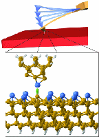
value / price ratio on the market combined with the famous German quality;- A possibility to visualize features below the surface is being developed using the idea published in a paper in "Science" in 2005. When implemented there will be an easy upgrade path;
- Both dynamic (tapping mode) and contact mode of operation;
- Large range of experimental methods: topography (AFM), friction (Friction Force Microscopy), magnetic forces (Magnetic Force Microscopy), electrical forces (Electrical Force Microscopy), elasticity of the substrate (Phase contrast imaging), capacity (Scanning Capacitance Microscopy), surface conductivity (Conductive AFM), work function (Kelvin Probe Force Microscopy (KPFM)). Anfatec are worldwide leaders in KPFM. Electrochemistry cell is under development.
- Built-in 3 levels of vibroisolation, which eliminates the need for additional vibroisolation: simple antivibration table, granite base plate, body hangs on rubber bands—the most effective vibroisolation according to scientific papers;
- 3 motors for leveling the sample. This greatly increases the number of samples that can be viewed without additional preparation and represents the newest trend in AFMs;
- Lateral resolution is limited by the fact that measurements are made in ambient air. Achievable lateral resolution in air < 5 nm. Technical resolution < 0.2 nm;
- Achievable vertical resolution < 0.1 nm (atomic steps). See the Si (111) figure above for example;
- One of the fastest control electronics on the market. Data refresh rate—40 kHz, bandwidth of the amplifiers7—over 700 kHz;
- Scan range (typical) on X and Y-48 µm, on Z-8µm. Manual sample positioning with precision screws—6 mm;
- Hardware (on all 3 axis!) and software linearization of the scanner;
- Possibility to gather data with high resolution: up to 2048 x 2048 points on all 8 channels;
- Built-in video camera with focusing optics and two levels of illumination;
- Two built-in dual phase low-noise lock-in amplifiers with more than 1 MHz bandwidth;
- Possibility to collect and visualize data on up to 8 channels simultaneously;d
- 15 step by step student exercises with samples to measure;
- The control software is with open license and the source code is freely distributed. Amendments to the software can be made by the manufacturer upon request. Free upgrade to newer versions. The possibility to adapt the software to different languages is currently being implemented.
- Powerful analyzing software is implemented. It has the possibility to do 3D visualization and rotation of the image, filtering and up to 2D leveling, calculations (e.g. roughness), picture optimization, etc. Inexpensive additional licenses so you can make demos on your laptop for example.
- The price includes a number of cantilevers (depending on system ordered);
- Included is a powerful low-noise desktop computer with two 19" LCD monitors;
- Two years of warrant
 |
A very difficult sample to measure. A monolayer from 30 nm ferrite spheres covered with oleic acid, deposited on a Si wafer. Measured in dynamic mode with sharpened tip. Measurement was done in a conference environment without the vibration isolation table. Individual spheres can clearly be seen. As well as some tree like aggregation of a bigger size spheres. Same sample in same environment was measured by a top of the line competitor's instrument costing over 160 000 € but did not reveal a better picture. See end of page. |
Some more images:
Si(111) steps measured with the Anfatec Level AFM. Scan size 1 x 1 µm2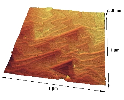 The sample preparation has been done in the Hahn-Meitner-Institute Berlin by Dr. Heike Angermann. The crucial point is a final removal of the SiO2 with Ammonium Fluoride, which enables the flat terraces. |
Atomic Force Microscopy and Magnetic Force Microscopy of a magnetic disk.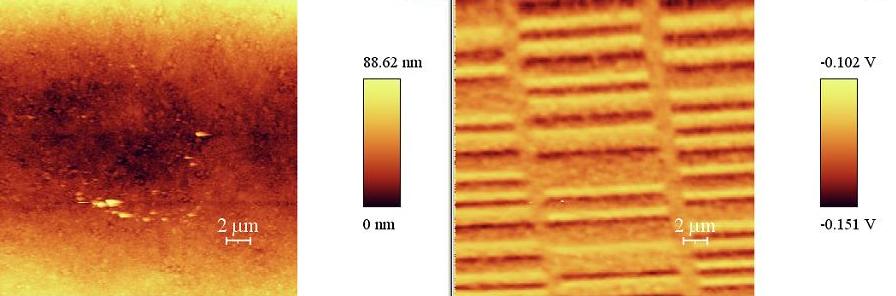 On the left is the AFM image which shows smooth surface. On the right is the MFM image which shows the recorded data bits. |
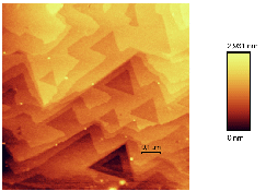
Porous anodic alumina. Height scale 0–940 nm.Sample courtesy MPI f. Mikrostrukturphysik Dr. Mato Knez 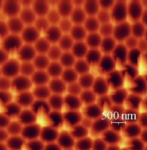 |
|
75 nm Alqb on silicon. Height scale 07ndash;47 nm.Sample courtesy TU Braunschweig. 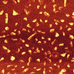
|
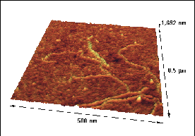
Biological Applications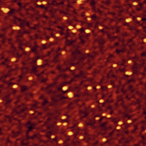 DNA functionalized gold particles deposited on gold surface. 1µm2 scan. Height scale 0–32 nm. |